
LayTec AG products
In-Situ Metrology
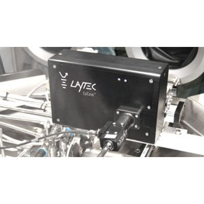
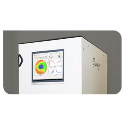
LayTec - Model EpiTT - Combines Measurements Instruments
EpiTT combines measurements of temperature and reflectance at three wavelengths in one tool. For True Temperature (TT), we apply the method of Emissivity Corrected Pyrometry, which delivers the precise surface temperatures of opaque materials at 950 nm (Si, GaAs, InP). For materials that are transparent at 950 nm (GaN, Sapphire, SiC), EpiTT measures the temperature on the top side of the carrier. Measuring reflectance at three wavelengths monitors all essential properties of the growing layers, such as growth rate, film thickness, stoichiometry changes and morphology.
LayTec EpiCurve - Model TT - Wafer Curvature Measurements System
To overcome the challenges that occur with larger wafers (4`, 6` or 8`), you need the advanced EpiCurve® TT system. It combines wafer curvature measurements with all the features of the EpiTT: emissivity-corrected pyrometry and growth rate/thickness measurements by three-wavelength reflectance. This tool will help you avoid cracks, achieve flat wafers and control temperature homogeneity. Every curvature tool can be equipped with Advanced Resolution (AR) curvature measurements for wafer bow asphericity control (EpiCurve® TT AR).
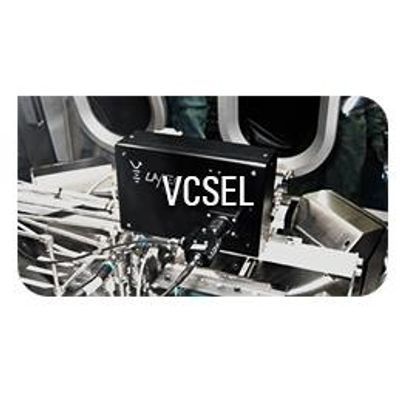
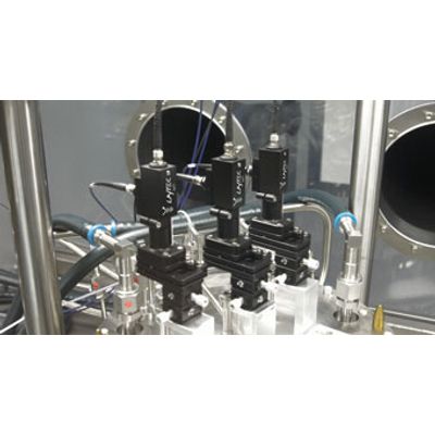
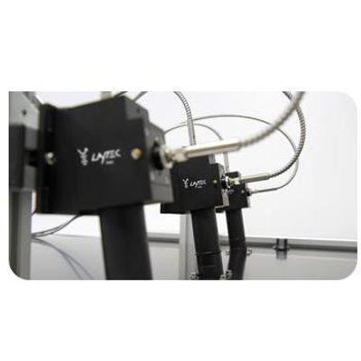
LayTec - Spectral Systems
ayTec has customized and expanded EpiTT`s performance for VCSEL epitaxy: The new EpiTT VCSEL combines spectral reflectance measurements with the robust and industry proven EpiTT performance. EpiTT VCSEL contains two fiber optical heads: one for a standard EpiTT and one for spectral reflectance sensing.
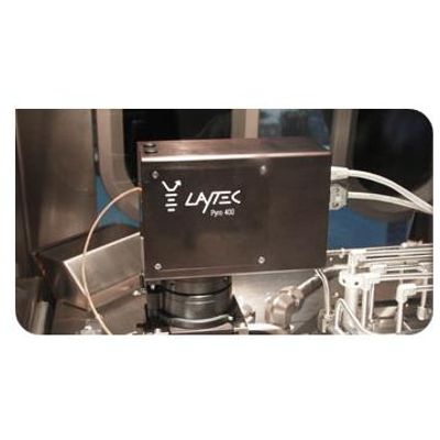
Pyro - Model 400 - Metrology System
LayTec offers an ultimate solution for GaN-based LED production: the Pyro 400 metrology system. It provides precise real surface temperature measurements during epitaxial growth of GaN on sapphire or SiC, and enables direct growth control of InGaN multiple quantum well (MQW) layers. While conventional pyrometers measure pocket temperature instead of wafer temperature, Pyro 400 provides both ultraviolet (UV) pyrometry for direct GaN surface temperature control and, additionally, infrared (IR) pyrometry for pocket temperature.
In-Line Metrology
LayTec PearL - Monitoring Analyzes System
The PearL monitoring system analyzes the spectrum of photoluminescent radiation emitted from a probed surface after excitation with laser light. It is designed for in-line integration in production lines. Spectroscopic photoluminescence (sPL) gives access to information on the band gap, electronic defects and the related composition of materials, e.g. the gallium / (gallium+indium) ratio (Ga/(Ga+In) ratio) and copper (Cu) content of CIGS solar cells. LayTec’s sPL has a total measurement and analysis time of only 100 ms.
EddyCus - Model TF - Inline System
The EddyCus® TF inline system offers contact-free real-time monitoring of deposition processes of thin-films, e.g. transparent conductive oxides using high speed eddy current measurement. It applies the method of Eddy Current Sensing and provides comprehensive conductivity/sheet resistance analysis. The system characterizes all conductive thin films including zinc oxide (ZnO), indium tin oxide (ITO) and other TCOs.
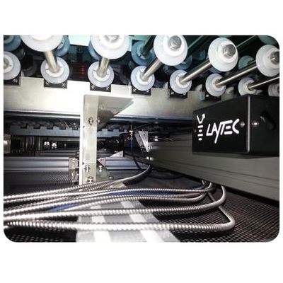
LayTec Flames - Multi-Head Optical Metrology System
LayTec Flames is a multi-head optical metrology system for monitoring multi-layer thin-film structures in large area processes. It measures multi-traces of layer thickness, reflectance, and transmittance uniformity directly after the deposition in in-line processes with thickness resolutions down to less than 1 nm.
At-Line Metrology
LayTec EpiX - Mapping Stations
EpiX Mapping stations combine an XY-mapping stage with LayTec spectroscopic reflectance and photoluminescence metrology systems for a comprehensive 2D analysis of optical wafer properties by non-contact measurements. Integrated software provides full automated data analysis, including detection of VCSEL optical parameters (cavity dip, stop-band position), single layer and multiple layer thickness fits, film composition and multiple-peak analysis. Moreover, customers benefit from sample’s statistics and pass/fail classification on wafer-level and die-level.