

- Home
- Companies
- TERA-print, LLC
- Products
- TERA-Fab - Model E series 2.0 - Beam ...
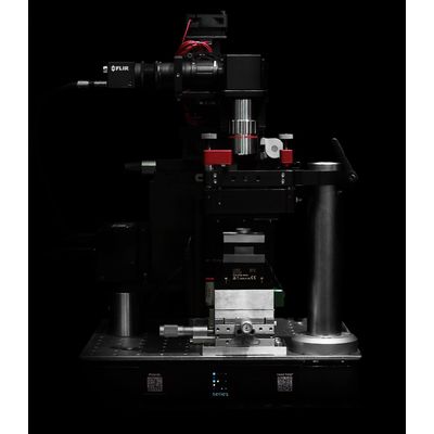
TERA-Fab - Model E series 2.0 -Beam Pen Lithography (BPL) System
High-resolution maskless photolithography.
Precise Multiwavelength Optics
Powered by an advanced light engine, the E series delivers high powered light with unparalleled uniformity across the projection area at the wavelength you need. Customize your E series by choosing from a range of LED options that span from UV to visible wavelengths.
Sub-Diffraction Limit to Micro Scale Resolution
Create patterns and structures with sub-diffraction resolution (<250 nm) by operating the E series in the beam pen lithography mode. Alternatively, access microscale resolution patterning (>1.25 µm) by using E series as a maskless photolithography tool without a beam pen array.
An Intelligent Digital Photomask Platform
Take advantage of our maskless pattern design platform and gain the ability to conduct truly arbitrary nano-and-micropatterning over mm2 to cm2 areas. By simply uploading an image (PNG, JPG, BMP), users can change their pattern design on the fly.
Efficient Automated Alignment
The E series features a fast and automated alignment function that enables repeatable and highly uniform patterned surfaces from one experiment to the next.
Control With Simplicity
Simple and intuitive hardware and software design allows users of any background to nanofabricate with E series after only a few hours of training. The eOS software provides full control over key patterning parameters that can be tailored for any application.
Team TERA, At Your Service
We take pride in our ability to serve our global user base with both on-site and virtual support. Team TERA is actively engaging with customers to ensure the best possible user experience.
Microfluidic Devices
Rapidly prototype microfluidic channel molds using conventional positive or negative photoresists right from your desktop.
Bioengineering
Generate complex hydrogel scaffolds via extracellular matrix (ECM) photopolymerization to create in vitro platforms with sub-cellular resolution.
Grayscale Lithography
Pattern complex features with 8-bit depth using dynamic exposure and reduced light intensity.
And many more.
Sample Control
Piezo X-Y-Z scan range (closed loop): 100 μm x 100 μm
Piezo X-Y-Z resolution (closed-loop): 1 nm typ.
Repeatability: <10 nm typ.
Manual X-Y positioning stage: 12.7 mm x 12.7 mm travel range
Motorized Z positioning: 12 mm travel range, bi-directional repeatability, 0.75 μm bidirectional repeatability, 2 mm/s maximum speed
ΘX and ΘY 2-axis angular positioning: ±12600 arcseconds angular range, 0.144 arcseconds angular resolution
Optics Control
Motorized X-Y motion: 35 mm x 35 mm travel range, bi-directional repeatibility: 1 μm
Motorized Z positioning: 50 mm travel range, bi-directional repeatibility: <50 μm, maximum speed: 3.0 mm/s
Digital Light Processing (DLP): DLP5500 1024 x 768 resolution
Light Sources: UV LED Light Engine (405 nm) 2.4-2.8 W, Green LED Light Engine (532 nm) 2.5 W, additional 460 nm and 365 nm options available
5x Objective M Plan APO: 34 mm working distance, 2 μm resolving power, additional objective lenses available (10x, 20x, 50x)
Field of View: 1.48 mm x 1.11 mm (with 5x objective installed)
CMOS camera: 12 MP (4000 x 3000), 0.74 cm x 0.56 cm sensor size, 1.85 μm x 1.85 μm pixel size
Features
- Achieve feature sizes from 250 nm to >100 μm
- Real-time force feedback for monitoring contact force throughout the experiment
- Automated electrical alignment procedure
- Live imaging of patterning process and low-resolution sample analysis
- Easy to access noise isolation enclosure
Software
X-Y-Z piezo scanning stage
- Set movement speed for each axis individually or all axes within a 1-100 μm/seconds range
- Move each axis individually or all axes to an absolute position or relative to current position within 100 μm range
Z positioning of sample stage
- Set movement speed of the long travel Z motor in a 0 to 2 mm/s range
- Move sample stage to an absolute position or relative to current position within 25 mm range
- Tilt pen array in ΘX and ΘY directions by a specified angle with a minimum increment of 4x10⁻⁵°
Stage leveling
- Automated pen array engagement with a substrate
- Real-time 4 corner contact monitor for manual alignment of pen array to the substrate plane
- Automated alignment of pen array to the substrate plane with our patented feedback-controlled algorithm
Patterning
- Creation of orthogonal dot patterns
- User specified dot spacing, dwell time, light exposure time, light patterns, and patterning speed
- Ability to save, load, and merge generated orthogonal patterns
- Pattern preview window
- Capability to define a custom pattern by loading an image; automatically generated sequence of patterns; user specified dot spacing, light exposure time, and patterning speed
Optics
- Integrated digital zoom control
- Integrated light intensity control
- Ability to control the illumination area by specifying the number of active DMD mirrors