
- Home
- Companies
- Hitachi High-Tech Analytical Science
- Products
- Hitachi High-Tech - Model Coating ...
Hitachi High-Tech - Model Coating Thickness Handheld Gauges -for PCB & Copper Surface
Our thickness gauges provide reliable, simple and accurate measurements. Choose from a range of digital coating thickness gauges that provide increasing functionality from the entry level models, to top of the range.Measuring printed circuit board copper thickness enables manufacturers to ensure boards meet tight specifications. Our full range of non-destructive coating thickness gauges allows you to verify foil and laminate thickness as well as copper thickness for plated through-hole and surface mount technology, including pads and traces.
Perform incoming inspection and process control using our PCB copper gauges for reliably to consistently produce high quality boards.
Common measurement applications with these digital PCB & copper surface gauges include
Copper foil and laminate thickness
Surface copper thickness
Through-hole copper thickness
QUALITY ASSURANCE FOR PCB FOIL AND LAMINATE COPPER THICKNESS AT INSPECTION AND BOARD FABRICATION
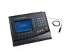
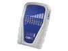
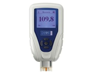
Measure foil or laminate thickness on PCBs between 1/8 to 4.0 oz/ft2 (5 - 140 μm) in less than 1 second. Our CMI95M® is easy to use – just place the unique soft-touch probe on the copper surface and note the thickness measurement on the indicator. This gauge uses field-proven microresistance technology to sort copper foil and laminates by thickness. The CMI95M® is robust, affordable and highly accurate. Because it is factory calibrated it does not require the use of standards. Common applications for the CMI95M® are:
| PCB manufacturing and assembly.
| Copper surface thickness.
KEY FEATURES:
| Battery operated with low battery warning.
| CE approved.
| Factory calibrated.
| Proven durability.
| Simple to use.
| Exclusive soft touch probe.
ACCURATE IN-PROCESS INSPECTION RESULTS REGARDLESS OF COPPER TEMPERATURE
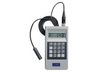
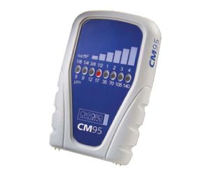
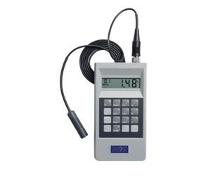
Temperature can affect the measurement on a copper sample. Our CMI165® can compensate for the temperature to produce accurate in-process inspection results regardless of the tempature of the copper. It is an ideal gauge for quality assurance and inspection for:
| PCM manufacturing and assembly.
| Copper surface thickness.
Our CMI165® gauge is versatile and portable. It comes equipped with a protective case and its durable design can be taken into the harshest environments. The CMI165® is a good choice to:
| Measure Cu on hot or cold PCBs.
| Reduce waste by eliminating the need for coupons.
| Measure Cu thickness on foils or laminates in μm, mils or oz.
| Sort Cu by weight at incoming inspection, prior to drilling, shearing or plating.
| Quantify Cu thickness after etching or planarizing.
| Verify Cu plating thickness on PCB surfaces.
| Measure thin etched traces down to 204 μm without use of standards.
KEY FEATURES:
| Temperature compensation.
| Durable design.
| Proprietary SRP-T1 replaceable probe.
| Illuminated probe tip for easy positioning.
| User interface in English or Simplified Chinese.
RAPIDLY MEASURE PLATED THRU-HOLE COPPER THICKNESS PRIOR TO, AND AFTER ETCHING
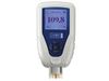
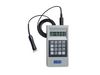
The CMI511® has an exclusive temperature compensation feature for in-process thickness measurement to reduce scrap and costly rework. Its automatic temperature correction makes it highly accurate even for measurement on boards that have just been lifted from the plating tank.
This gauge is an ideal choice for:
| PCB manufacturing and assembly.
| Thru-hole copper thickness.
The CMI511® does not require standards because it factory calibrated ensuring its performance is always highly accurate. It is ideal for double-sided and multilayer boards, even plated with tin and tin/lead. The CMI511® provides instantaneous measurements, and is so easy to use that no operator training is necessary. Our CMI511® comes complete with a carry case that features a plastic window which allows use of the gauge even without removal from the case.
KEY FEATURES:
| Simple to use.
| Temperature compensation for accuracy right out of the bath.
| Multi-layer measurement.
| Factory calibration.
| Battery operated.
| Multi-layer measurement.

MICRORESISTANCE TECHNOLOGY FOR ACCURATE MEASUREMENT OF SURFACE COPPER
The CMI563® provides advanced technology for accurate measurement on copper plating and it ensures that the opposite side of the PCB will not interfere with readings, regardless of laminate thickness. Our CMI563® makes it simple to obtain precise surface copper measurement on laminate, electroless, or electrolytic copper.
This gauge is an ideally suited for:
| PCB manufacturing and assembly.
| Copper surface thickness.
Our CMI563® provides superior performance for copper foil measurement on flexible or rigid, single, double-sided, or multi-layer boards.
KEY FEATURES:
| Advanced microsistance technology.
| Factory calibrated.
| Highly accurate copper thickness measurement.
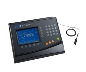
TEST FOIL, LAMINATE, SURFACE, TRACES AND THRU-HOLE
COPPER WITH A SINGLE DEVICE
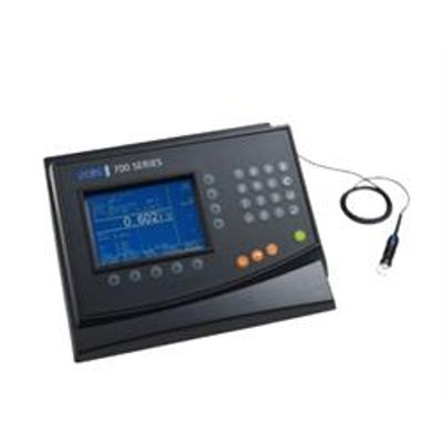
The CMl760® accepts multiple probe types to meet almost any PCB application, including surface copper, and through-hole applications. Our CMl760® comes standard with the SRP-4 probe and an advanced statistical package for interpretation of test data. This instrument is highly-expandable, capable of both micro-resistance and eddy current testing for the accurate and precise measurement of copper. Optional accessories are available to measure thru-hole copper thickness.
SRP-4 PROBE
The CMI760® includes a tethered SRP-4 Probe with user-replaceable tips for added convenience and its more cost effective. This probe consists of four pins encased securely in a patented design for durability and resistance to breakage and wear. A see-through casing allows for easy placement of the probe on small traces. The tethered cable is ideal for field applications plus its small footprint is convenient and user-friendly.
OPTIONAL ETP PROBE
Using our ETP Probe the CMI760® operates with eddy current. This probe generates accurate readings regardless of the board’s multiple layers, working equally well on double-sided and multilayer boards, before and after etch, even with tin and tin/lead resist. It also provides a temperature compensation feature, for measurement of the board immediately after it is lifted from the plating tank.
KEY FEATURES:
| Dual technology – eddy current and microresistance.
| Surface and thru-hole probes.
| Active statistical display.
| Optional foot switch.