

imec - Silicon Photonic ICs for Prototyping and Volume Production
Imec offers an integrated silicon photonics platform targeted to the telecom, datacom and medical diagnostics industries: our silicon photonics platform (iSiPP).
The iSiPP platform co-integrates a wide variety of passive and active components, enabling competitive photonic integrated circuits for short reach optical interconnects.
Get access to small-volume manufacturing and prototyping by leveraging imec`s mature iSiPP50G platform through imec.IC-link`s MPW service. And volume production thanks to our strategic partnership with SilTerra.
Imec`s iSiPP platform is SOI-based and comes in three distinct flavors:
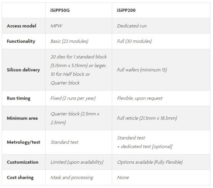
- iSiPP200: 200mm (8”) full platform (see table below)
- iSiPP50G: 200mm (8”) simplified platform/flow (see table below)
- iSiPP300: options with TSV (through silicon via), microbumps and embedded microbumps are available in a 300mm (12”) platform
In 2023, imec`s silicon photonics platform received an important upgrade through the co-integration of its high-quality silicon nitride waveguide technology – without performance degradation of the high-bandwidth active devices.
Also, together with III-V expert Sivers Photonics and equipment supplier ASMPT, imec succeeded in developing flip-chip bonded InP lasers on silicon photonic ICs, at wafer scale.
Thanks to the strategic partnership of imec with SilTerra, you can process advanced silicon photonic circuits designed in imec’s PDK, in large volumes in a commercial 200mm foundry. And insert state-of-the-art add-ons that are only available at imec – because of the wafer exchange between imec and SilTerra.
Building blocks that are available for this technology transfer include:
- 193nm lithography-based multi-level silicon patterning
- Si p-n diode phase shifters for high-speed Mach-Zehnder and ring modulators
- Ge photodetectors
- W heaters with optional substrate undercut
- 2 levels of Cu metal interconnect
- Si, SiN or SiON edge couplers
- encapsulated local substrate undercut
- Starting substrate: Silicon-on-insulator with 220nm Si / 2000nm BOX
- 3-level Si & 1-level poly-Si patterning with 193nm lithography
- 6-level silicon doping & 2-level Ge doping
- Ge-on-Si RPCVD epitaxy
- 2-level Cu interconnects + Al bondpad
- Deep-Si etch for edge coupling
- Traveling–wave Mach-Zehnder p-n modulator
- Ge(Si) electro-absorption modulator
- Micro-ring p-n modulator
- Waveguide-based Ge-on-Si detectors
- Fiber coupling:
- Vertical “raised” grating
- C-band edge coupler
- Passive waveguide-based devices such as filters
- Integrated heaters