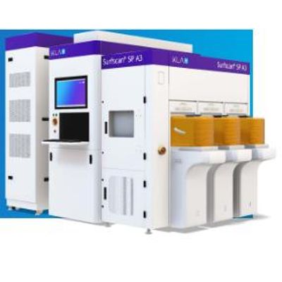
KLA - Model Surfscan SP Ax -Unpatterned Wafer Defect Inspection System
The Surfscan SP A2 and Surfscan SP A3 unpatterned wafer inspection systems identify defects and wafer surface quality issues that affect the performance and reliability of chips manufactured for the automotive, IoT, 5G, consumer electronics, and industrial (military, aerospace, medical) applications.
These inspection systems support device, OEM, materials and substrate manufacturing by qualifying and monitoring tools, processes and materials. Using a DUV laser and optimized inspection modes, the Surfscan SP Ax systems deliver the sensitivity required to support fabs defect reduction strategies. Standard darkfield and optional brightfield inspection modes run concurrently, enabling capture and classification of yield critical and latent reliability defect types. Built on the industry-leading Surfscan platform, the Surfscan SP A2/A3 inspectors are configurable and flexible to meet the cost and performance targets for a range of applications. They support substrate and device manufacturing based on either silicon or wide bandgap (SiC, GaN, etc.) materials across 150mm, 200mm and 300mm wafer sizes.
- Process qualification, Tool qualification, Tool monitoring, Outgoing wafer quality control, Incoming wafer quality control, Process debug