
- Home
- Companies
- KMLabs Inc.
- Products
- KMLabs - Model QM - Quantum Microscope
KMLabs - Model QM -Quantum Microscope
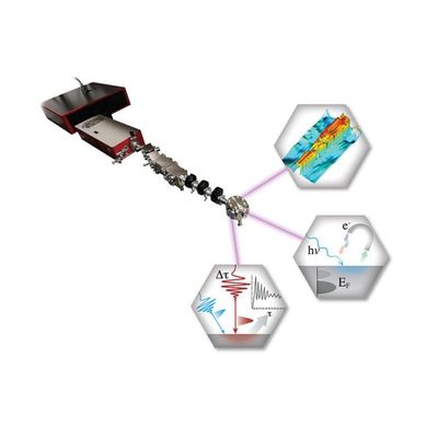
KMLabs QM Quantum Microscope advanced photon imaging solution is a fully integrated, commercialized platform enabling ultrafast spectroscopy in the EUV range and high-contrast, near surface-to-subsurface imaging at the nanoscale. It enables laboratory-based 2D high contrast imaging of composition and structure, study of mechanical properties of patterned films, deep understanding of materials properties, and functional characterization of spintronic, ALD, 2D, low-density lightweight, energy, space and photovoltaic materials.
Interested in how the Quantum Microscope platform might be useful for semiconductor applications? Check out this video from former JILA graduate student Kathy Hoogeboom-Pot:
A suite of integrated systems developed to elucidate critical details of critical technology problems.
By combining the time sensitivity of femtosecond lasers with the spatial resolution of EUV microscopy and diffraction, QM enables a series of techniques tuned for important challenges in research and industry. E.g., for batteries, EUV absorption near the lithium edge provides a microscopic and spectroscopically rich area to understand lithium bonding. For semiconductors, QM provides critical detail on buried and surface nanotopography with unique sensitivity to bonding.
Completely configurable, the QM Quantum Microscope comprises a laser source (EUV and/or VUV), amplifier, beamline tailored to the user’s experiment, and imaging or other analysis workstations that can effectively cover the microscopy/spectroscopy landscape for nano-to-quantum materials.
- Non-destructive imaging brings time-resolved research to nanometer length scales
- Uniquely capable of topographical surface imaging (biological, semiconductor, quantum)
- One or more beamlines with endstations can be configured to your requirements
- Diffraction for nanometer-scale order in self-assembled materials
- Structural pump probe for mechanical and thin-film property evaluation to understand elasticity response, thermal transport, and phonon modes
- High resolution, revolutionary measurement of magnetic systems is highly sensitive to different magnetic layers
- Coherent diffraction imaging (CDI)
- Pump probe spectroscopy
- Magnetic dynamics
- ARPES
- MOKE diffraction and magnetic imaging
- Reflectometry
- Magnetic imaging at band edge
- IR pump/EUV probe diffraction imaging for thermomechanical and elastic data
- High speed spin transport dynamics
- Integrated, high performance ultrafast EUV laser source
- High resolution interferometric surface and subsurface imaging
- x/y spatial resolution to <20 nm
- Multiuse beamline with configurable endstations
- Pump probe (XUV pump/IR probe) designs
- Extensible to VUV (60 - 150 nm or 8.3 to 20.7 eV)