

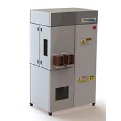
MetroThick - Model 201 -Film Metrology System
The MetroThick 201 film metrology system helps achieve strict process tolerances at sub-7nm logic and leading-edge memory design nodes by providing high-precision thin film measurements for a broad range of film layers. The high brightness light source drives the spectroscopic ellipsometry technology which provides the signal required to accurately measure the bandgap and provide insight into electrical performance weeks earlier than e-test. New FoG™ (Films on Grating) algorithms further increase the measurement’s correlation to device by enabling film measurement on a device-like grating structure. With increased throughput, MetroThick 201 offers high productivity, supporting the increased number of film layers associated with leading-edge device fabrication techniques.
- Measures Thickness & Refractive Index of Single & Multi Layer Films.
- For control of advanced film processes at the 65nm and 45nm.
- Uses spectroscopic ellipsometry (SE) technology .
- Non-destructively measures in-die process variation.
- Uses Dielectric Pattern Metrology (DPM), advanced resolution optics,vacuum ultraviolet (VUV) 150-nm SE.
- Provides Spectroscopic Ellipsometry from 230nm .
Diffusion Films
Complete diffusion solution in AccuFilm and SE technologies for ultra-thin gate oxides, shallow trench isolation, gate anti-reflective coating (ARC) layers, hard masks, SOI substrates, and SiGe stacks.
Chemical Vapor Deposition (CVD)
SE and DBS measurement capabilities cover a wide range of thicknesses and indices with a single recipe for multi-layer ARC, hard mask stacks, and copper dual damascene low-k stacks.
Chemical Mechanical Planarization
Unique capability to determine transparent film thickness on a metal array. Industry’s smallest SE measurement area enables post-cu CMP dielectric stack measurements. Best-in-class robust pattern recognition and auto model select features are an added advantage, especially for CMP processes such as post-STI, post-copper CMP, and post-interlayer dielectric polish monitoring.
Lithography
SE and DUV spectrometry technologies, with wavelength range down to 190 nm, determine critical lithography measurements for photoresist and ARC thickness and refractive indices needed for advanced 193 nm resist development, ARC layer characterization, and process control.
Etch
SE technology allows precise and stable measurements on post-poly-gate, STI trench, dielectric via, and trench etch. SE also has the capability to compensate for surface roughness, which enables more accurate and precise RI measurement for etch to thin films.
Metals
SE technology also allows production-worthy measurement of ultra-thin physical vapor deposition, CVD, and ALD metal stacks with high optical extinction coefficients such as Co and Ni salicides, thin Ti/TiN liner/barriers, copper barriers, Ta, TaN/Ta, and TiSiN.