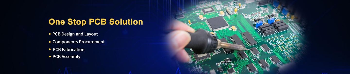

Printed Circuit Boards (PCB) are an integral part of almost all electronic applications. Without PCBs the electronics industry can’t manufacture products. But what manufacturing techniques make these PCBs robust enough to hold circuits and run them smoothly? On commercial scale, PCB manufacturing is quite detailed and involves extensive use of technical procedures.
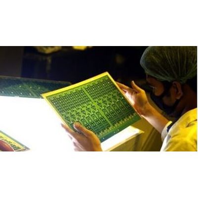
The Multi layer PCB manufacturing process starts with Computer Aided Design (CAD) of the circuit, later, this design is printed on to the PCB and the copper layers are removed from unwanted regions. The board is drilled for through-hole components. Later the board goes through testing and once clear, it is ready for component assembling. The procedure varies depending upon the type of PCB and components.