- Home
- Companies
- Silicon Valley Microelectronics, Inc. ...
- Products
- SVM - Silicon on Insulator Wafers (SOI ...
SVM - Silicon on Insulator Wafers (SOI Wafers)
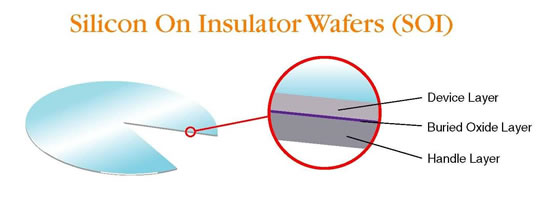
Most commonly used in MEMS and advanced CMOS integrated circuit fabrication, SOI wafers provide a manufacturing solution which helps reduce power and heat while increasing the speed performance of a device. SOI wafers are a three layer material stack composed of the following: Active layer of prime quality silicon (DEVICE LAYER) over a buried layer(BOX) of electrically insulating silicon dioxide, over a bulk silicon support wafer (HANDLE). SOI wafers are unique products which are custom built for specific end-user applications. SVM offers two types of SOI: Thick Film and Thin Film.
Thick Film
- Material: Silicon
- Wafer Diameter: 76.2mm (3”) to 200mm (8”)
- Type/Dopant: N or P
- Device Layer Thickness: >1.5um
Thin Film
- Material: Silicon
- Wafer Diameter: 150mm (6”), 200mm (8”), 300mm (12”)
- Type/Dopant: N or P
- Device Layer: >20nm (0.02um)
- Cz and Fz grown silicon SOI
- Single side polish and double side polish
- Prototype and production volumes
- Consistent, reliable production supply line
- Competitive pricing
- Excess inventory
SVM is currently carrying excess inventory of the following Thick Film SOI wafer specification:
Silicon SOI wafer
- Diameter: 150mm
- Orientation: <100>
- TTV: <8um
- Bow/Warp:<30um
- Front Surface: Polished
- Back Surface: Etched
DEVICE Layer:
- Type/Dopant: N/Phos
- Resistivity: 1-5 ohm-cm
- Thickness: 2-3um
BOX Layer:
- Thickness: 1um +/-0.1um
HANDLE wafer:
- Type/Dopant: P/Boron
- Resistivity: 10-20 ohm-cm
- Thickness: 625+/-15um