
PCB - System-in-Package (SiP) Technology
Advanced Packaging is a blanket term used to describe a general grouping of various distinct methodologies. Advanced Packaging technologies include: 2.5D, 3D, Fan-Out (2D), Wafer Level Packaging and System-in-Package (SiP). SiP is a combination of multiple active electronic components of diverse functionality, assembled in a single unit, that performs multiple functions associated with a system or sub-system.
SiP may optionally contain passives, MEMS, optical components and other packages or devices; including a combination of bare dies and SMT components.
SiP is designed to be a complete system within a single package, whereas a Multi-Chip-Module (MCM), containing two or more interconnected chips, isn’t necessarily a complete system.
Advanced Packaging Technologies
- SiP / MCM Packaging
- Heterogenous Integration
- 3D / 2.5D Packaging
2D Packaging = Integration method of mounting 2 or more dies horizontally on the surface of the substrate:
Takes up less space and provides more functionality compared with SMT
CTE matching, reinforced structure, good thermal dissipation solution
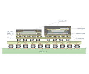
2.5D Packaging = 2 or more active semiconductor chips placed side-by-side on a silicon interposer for extremely high die-to-die interconnect density:
Takes up less space than 2D, when using high IO dies
Improved thermal and CTE matching
Reinforced structure
3D Packaging = Multiple layers/chips/wafers, stacked vertically and electrically interconnected, to enable die-on-die and package-on-package solutions:
Optimizes functionality
Superior system design featuring thermal, CTE and structural advantages