
- Home
- Companies
- Thermo Fisher Scientific, LIMS & ...
- Products
- Talos - Model F200E TEM - Transmission ...
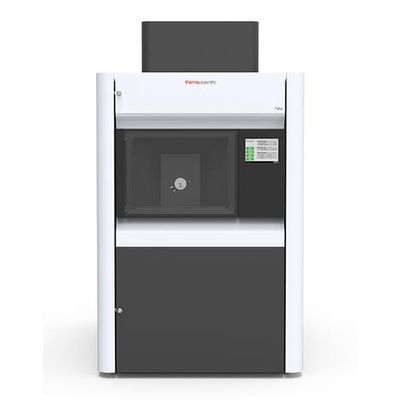
Talos - Model F200E TEM -Transmission Electron Microscopes
200 kV TEM and STEM for repeatable, high-volume analysis of a broad range of semiconductor and microelectronic devices.
Demand for faster, smaller, and more interconnected devices continues to drive atomic scale technology developments. Researchers and engineers need reliable and rapid analysis and characterization at these dimensions, which only transmission electron microscopy (TEM) can provide.
The Thermo Scientific Talos F200E (Scanning) Transmission Electron Microscope provides high-resolution STEM and TEM imaging with minimal distortion, combined with high-throughput energy-dispersive X-ray spectroscopy (EDS) functionality, tailored for a wide range of semiconductor defect analysis and research applications.
A high-productivity solution for semiconductor and microelectronics analysisSupporting the fast pace of process development and yield ramp significantly strains semiconductor analysis labs, as they must provide repeatable, high-resolution characterization of a wide variety of materials and devices. The Talos F200E (S)TEM was designed with these labs in mind, delivering >1.5× faster EDS analysis compared to previous Talos models and ≤1% TEM image distortion. The speed and repeatability improvements make the Talos F200E (S)TEM the industry choice for device analysis, defect characterization, and yield support.
High-quality (S)TEM imaging
High-throughput TEM imaging with minimized distortion and simultaneous, multiple-signal detection, and contrast-optimized STEM imaging.
Precise, high-speed chemical characterization
Rapid, precise, qualitative or quantitative EDS acquisition and analysis.
Dedicated semiconductor-related applications
Includes: specimen-stage-synchronized live TEM image rotation, simultaneous operation of multiple STEM detectors, integrated differential phase contrast (iDPC) imaging, STEM field-of-view matching, instant EDS map quantification, minimized image distortion, and more.
- Camera: Low-distortion 4k × 4k with the Thermo Scientific Ceta-M Camera
- STEM: Panther STEM segment detectors
- SEMI S2: Certified
- STEM resolution: ≤0.16 nm
- TEM information limit: ≤0.12 nm
- TEM line resolution: ≤0.10 nm
- Max. diffraction angle: 24˚
- Z-movement: ±0.375 mm
- TEM image linear distortion: ≤1%
- TEM image variation(optional): ≤1%
- Gatan Continuum Filter: Optional
Semiconductor Failure Analysis
Increasingly complex semiconductor device structures result in more places for failure-inducing defects to hide. Our next-generation workflows help you localize and characterize subtle electrical issues that affect yield, performance, and reliability.
Physical and Chemical Characterization
Ongoing consumer demand drives the creation of smaller, faster, and cheaper electronic devices. Their production relies on high-productivity instruments and workflows that image, analyze, and characterize a broad range of semiconductor and display devices.