

Advantest America,Inc. products
IC Test Systems- SoC Test Systems
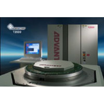
SoC - Model T2000 - Rapid Response Semiconductor Testing
SoC devices require small-lot high-mix manufacturing methods in the present era of rapid generation change. Semiconductor makers struggle with requirements to replace their testers on a 2-3 year cycle. The T2000 addresses their needs by enabling rapid response to market needs with minimum capital investment.

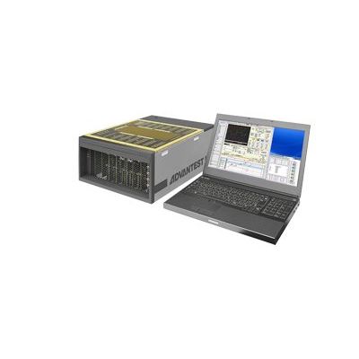
Advantest SoC - Model V93000 - Wave Scale Test System
Architecturally advanced cards provide the high parallelism and massive multi-site capabilities that allow customers to cost-effectively test the current and upcoming generations of communication devices. To remain on pace with the semiconductor technology advances leading to next-generation 5G wireless communications, testing capabilities for RF and mixed-signal ICs must reach new highs in parallelism and throughput. ADVANTEST’s Wave Scale generation of channel cards for the V93000 platform enable highly parallel multi-site and in-site testing that dramatically reduces the cost of test and ultimately the time to market for current and future devices.
IC Test Systems- Evolutionary Value Added Measurement System
Advantest - Model EVA100 - Analog / Sensor IC Measurement System
In recent years the number of smart devices we use has increased significantly. The role of the analog / sensor IC has become critically important not only in the smart society but also in other fields. More than ever, higher performance, tighter accuracy and longer reliability are required for those devices. To address these challenges measurement systems need to have many features while maintaining a very low test cost and engineers tasked with developing test programs require very good coding skills plus in-depth operation knowledge of the test system.
E-Beam Lithography
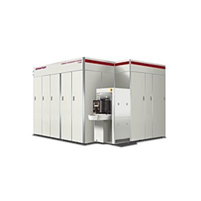
E-Beam - Model F7000 - Lithography System
The F7000 is an EB lithography tool with superior resolution performance meeting requirements for the 1Xnm technology node. The F7000 supports substrates of diverse materials, sizes, and shapes, including nano-imprint templates, as well as wafers, and is optimized for diverse applications such as advanced LSIs, photonics, MEMS, and other nano-processes. Also, users can select the configuration optimal for their needs, either stand-alone or in-line, enabling the F7000 to support a wide array of applications from R&D to volume production.
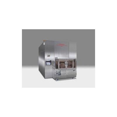
E-Beam - Model F5113 - Lithography System
Low-Cost, High Throughput EB Lithography Tool Supports Ultrafine Pattern Fabrication for Diverse Substrates. The F5113 is an electron-beam lithography system supporting 200mm and 3-inch through to 6-inch substrates, making it an optimal tool for processing advanced LSIs, compound semiconductor wafers, magnetic heads, smart power devices, photonics devices, MEMS, and other devices requiring ultrafine-pitch fabrication. The F5113`s character projection (CP) functionality offers high resolution, excellent pattern fidelity, and high throughput. High-speed pattern exposure with CP enables a broad range of applications, including materials R&D and evaluation. Advantest`s proprietary self-cleaning technology massively improves the stability of the electron beam used by the F5113, contributing to higher utilization ratios and lower customer running costs across the spectrum of applications.