

SENTECH Instruments GmbH products
Plasma Process Technology - Atomic Layer Deposition Systems
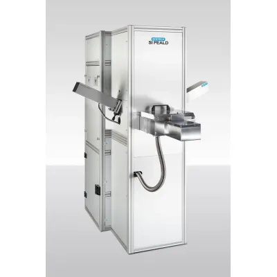
SENTECH - Model SI PEALD - PEALD System with True Remote CCP Source
The SENTECH SI PEALD system is designed for the homogenous and conformal coating of sensitive substrates and layers, operating efficiently at low temperatures under 100°C. This advanced atomic layer deposition technology ensures precise, conformal, and uniform film deposition, crucial for semiconductor applications like high-k dielectric materials. ALD systems by SENTECH offer in-situ diagnostics using the AL Real Time Monitor for optimized process development, enabling ultra-high resolution monitoring of single ALD cycles and spectroscopic ellipsometry for further analysis. The system allows for easy reactor cleaning with a lifting device and supports integration into SENTECH Cluster Tools and glove boxes. Compatible with a wide range of deposition types including oxides, nitrides, and 2D materials, SENTECH's systems also support both thermal and plasma-enhanced operation. Their flexibility and modularity underpin the combination of different ALD films into multilayer structures. The PEALD system emphasizes stability and repeatability in atomic layer deposition, offering comprehensive plasma deposition technologies from the nanometer scale upwards.
Thin Film Metrology - Spectroscopic Reflectometry
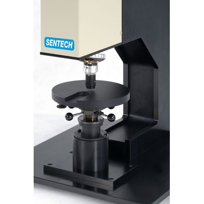
SENTECH - Model RM 1000 and RM 2000 - Spectroscopic Reflectometery Tools
SENTECH's RM 1000 and RM 2000 spectroscopic reflectometers are cutting-edge tools specifically designed for refractive index measurements and optical characterization of thin films. These instruments feature a precise single beam reflectance measurement mechanism, optimized through height and tilt adjustments and highly efficient light conduction optics. This ensures accurate and repeatable measurements, even on rough surfaces. The RM 1000 covers a spectral range from 410 nm to 1000 nm, whereas the RM 2000 spans from 200 nm to 1000 nm. Both models can be equipped with an optional x-y mapping stage and mapping software for high-resolution thickness mapping on microscale substrates. They support extensive material analysis capabilities, measuring film thicknesses ranging from 2nm to 100µm, and being versatile enough for applications in industries like microelectronics, optoelectronics, and biotechnologies. SENTECH’s proprietary FTPadv Expert software provides robust data acquisition, modeling, and automatic selection of sample models, making these reflectometers indispensable for advanced research and industrial applications.