SENTECH Instruments GmbH
  1. Companies
  2. SENTECH Instruments GmbH
  3. Products
  4. SENTECH - Model SI PEALD - PEALD System ...
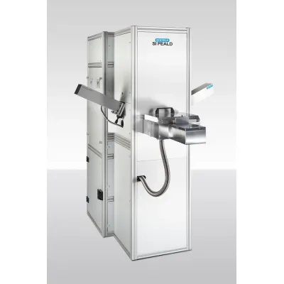
SENTECHModel SI PEALD -PEALD System with True Remote CCP Source

SHARE

The SENTECH SI PEALD system is designed for the homogenous and conformal coating of sensitive substrates and layers, operating efficiently at low temperatures under 100°C. This advanced atomic layer deposition technology ensures precise, conformal, and uniform film deposition, crucial for semiconductor applications like high-k dielectric materials. ALD systems by SENTECH offer in-situ diagnostics using the AL Real Time Monitor for optimized process development, enabling ultra-high resolution monitoring of single ALD cycles and spectroscopic ellipsometry for further analysis. The system allows for easy reactor cleaning with a lifting device and supports integration into SENTECH Cluster Tools and glove boxes. Compatible with a wide range of deposition types including oxides, nitrides, and 2D materials, SENTECH's systems also support both thermal and plasma-enhanced operation. Their flexibility and modularity underpin the combination of different ALD films into multilayer structures. The PEALD system emphasizes stability and repeatability in atomic layer deposition, offering comprehensive plasma deposition technologies from the nanometer scale upwards.

Most popular related searches
The SENTECH True Remote CCP Source enables homogenous and conformal coating of sensitive substrates and layers at low temperatures. A high flux of reactive gas species is provided at the sample surface without UV radiation or ion bombardment.
 

PEALD for sensitive substrates

The SENTECH SI PEALD system with true remote plasma source enables homogenous and conformal coating of sensitive substrates and layers at low temperatures <100 °C. A high flux of reactive gas species is provided at the sample surface without UV radiation or ion bombardment.

Atomic layer deposition (ALD) for precise, conformal, and uniform deposition

The ALD deposition technique is characterised by its ability to deposit conformal and uniform films with precise control over thickness at the atomic level and continues to play a growing role in semiconductor devices such as the deposition of high-k dielectric materials. Some of the primary applications of ALD include sensors, optoelectronics and 2D materials.

In-situ diagnostics for process development and optimisation

In-situ diagnostics by the AL Real Time Monitor enables ultra-high resolution of single ALD cycles. The advantages are confirmation of the ALD regime, reduction of process time, and total cost of ownership. Spectroscopic ellipsometry is provided as in-situ diagnostics, too, having specific advantages for our atomic layer deposition systems.

Easy reactor cleaning

Regular reactor cleaning is essential for stable and repeatable atomic layer deposition processing. The reactor chamber is easily opened with the help of a lifting device for cleaning our atomic layer deposition systems.

Cluster integration

Atomic layer deposition systems are available as modules for SENTECH Cluster Tools. Our atomic layer deposition systems can be combined with SENTECH PECVD and etch systems for industrial applications. Cluster tools optionally feature cassette-to-cassette loading.

Glove box system integration

SENTECH ALD Systems are compatible with glove boxes from various suppliers.