

- Home
- Companies
- Tescan Group, a.s.
- Products
Tescan Group, a.s. products
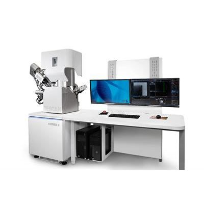
TESCAN - Model AMBER X - Plasma FIB-SEM System Solution
A unique combination of plasma FIB and field-free UHR FE-SEM for the widest range of multiscale materials characterization applications.
FIB-SEM
XEIA - Model 3 - High Resolution FIB-SEM Imaging System
Extraordinary ultra-high resolution imaging and extreme micromachining power in one single instrument. Whether your applications demand extremely powerful and ultra-fast micro-/nano- FIB machining, an ultimate uncompromised ultra-high resolution (UHR) at low beam energies, ultra-fast and reliable microanalysis or 3D analytical reconstructions, XEIA3 stands out as the ideal turnkey FIB-SEM system that offers all these capabilities in one single and unique instrument with outstanding performance. With the new XEIA3, TESCAN not only delivers an instrument top of its class but also fulfils its commitment to continue helping researchers push science and development forward. This is also reflected in the careful customisation of every system in order to meet the specific needs of every customer. From materials to life sciences or from engineering to the semiconductor industry, TESCAN guarantees high-per-formance systems without any compromises.
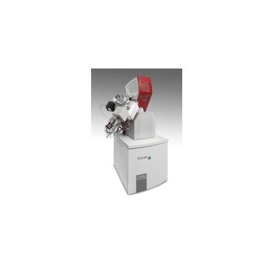
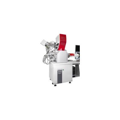
LYRA - Model 3 - Dual-Beam FIB-SEM System
TESCAN GAIA3 brings together an ultra-high resolution electron column and high-performance ion column fitted onto a single chamber. Built on the proven (MAIA3) FE-SEM platform, GAIA3 extends all of its qualities with the ability to modify surfaces with a focused ion beam. The outstanding imaging capabilities of the GAIA3 begin with its novel FE-SEM with excellent resolution at low voltages. The objective lens is narrower than a conventional objective and InBeam SE and InBeam BSE detectors placed in the column give free space over the sample for unlimited FIB work and various analytical techniques.
TESCAN - Model FERA3 - Scanning Electron Microscopes
The world’s first fully integrated Xe plasma source FIB with SEM enables extremely high ion currents up to 2 μA thus increasing sputtering rate more than 50 times compared to conventional Ga source. This predetermines FERA3 for milling big volumes of materials that were time consuming or impossible so far. This new generation of scanning electron microscopes equipped with focused ion beam column provides users with the advantages of the latest technology, such as new improved high-performance electronics for faster image acquisition, ultra-fast scanning system with compensation of static and dynamic image aberrations or built-in scripting for user-defined applications.
Detectors
TESCAN - Model SE - Secondary Electron Detectors
Secondary electrons (SEs) are low energy electrons emitted from a localised area at the uppermost layers of samples surface (within a range of a few nm depths); therefore, they provide high-resolution imaging suitable for detailed topographical characterisation of samples. SEs are produced when primary electrons from the beam interact inelastically with the specimen. SEs have energies of < 50 eV, however.
TESCAN - Model BSE - Backscattered Electron Detectors
Backscattered electrons (BSEs) are high-energy electrons generated as a result of elastic interactions between the primary electron beam and the sample. The range energy of BSEs is from 50 eV up to the energy of the electron beam. BSEs are emitted from a broad region within the interaction volume (the region in the sample where all the beam-sample interactions take place) with a range of penetration that can be as deep as a few microns for high-energy beams to hundreds or even a few tens of nanometres for low beam energies