

Tescan Group, a.s.
- Home
- Companies
- Tescan Group, a.s.
- Products
- TESCAN - Model FERA3 - Scanning ...
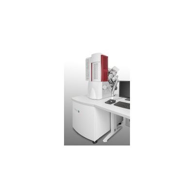
TESCAN - Model FERA3 -Scanning Electron Microscopes
The world’s first fully integrated Xe plasma source FIB with SEM enables extremely high ion currents up to 2 μA thus increasing sputtering rate more than 50 times compared to conventional Ga source. This predetermines FERA3 for milling big volumes of materials that were time consuming or impossible so far. This new generation of scanning electron microscopes equipped with focused ion beam column provides users with the advantages of the latest technology, such as new improved high-performance electronics for faster image acquisition, ultra-fast scanning system with compensation of static and dynamic image aberrations or built-in scripting for user-defined applications.
Most popular related searches
Modern electron optics
- The unique Wide Field Optics™ design with a proprietary Intermediate Lens (IML) offers a variety of working and display modes with enhanced field of view or depth of focus
- Real time In-Flight Beam Tracing™ for performance and beam optimization. Also includes direct and continual control of beam parameters.
- Fully automated electron optics set-up and alignment
- Rapid imaging with rates up to 20 ns
- Unique live stereoscopic imaging using the advanced 3D Beam Technology opens up the micro and nano-world for an amazing 3D experience and 3D navigation
Extremely powerful Xe plasma FIB column ECR-generated Xe plasma ion source FIB columnfor achieving the most challenging large-scale milling tasks in unbeatable short times frames
- 50x faster than Ga LMIS FIBs.
- Ion beam range current of 1 pA to 2 µA and resolution of < 25 nm
- Newly developed high resolution Xe plasma FIB column (Optional) achieving resolution of < 15 nm for extended patterning capabilities
- Large-mass xenon ions with larger FIB current range for ultra-fast sputtering even without gas-assisted enhancement
- Significant reduction in ion implantation compared to Ga LMIS FIBs
- Xe noble gas atoms do not alter electrical properties in the vicinity of the patterned area
- No intermetallic compounds formed during FIB milling