

- Home
- Companies
- SURAGUS GmbH
- Products
- EddyCus MA map (MPECS) - Crack, Flaw ...
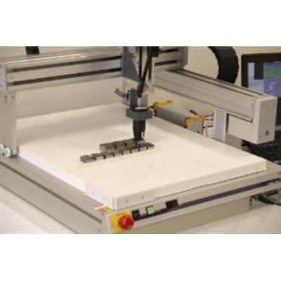
EddyCus MA map (MPECS) - Crack, Flaw and Surface Conductivity Mapping System
The system allows a fast, user-friendly mapping of the surface conductivity and surface defects of flat and curved samples. There are various sensors with different sensitivities and spatial resolutions customizes for different material systems available that are delivered with ready to use measurment receipies. SURAGUS also offers customized systems for specific testing tasks. The systems come with adapted parameter sets for definition of the scan area for each test material and parametrizing the eddy current sensors. The use of the system is very easy, the user places the sample, loads the measurement recipe, starts the measurement and obtains the eddy current high resolution images. Defect gets classified and results can be automaticly analysed and exported or transfed by a automated pdf report option.
Setups and Sensors
- Mapping of surface flaws, cracks and impurities of metals and alloys
- Mapping of the surface conductivity of metals and alloys
Characteristics
- Contact-free measurement or in sliding contact
- One to 25 test parts per run/scan (measuruements fiels and speciment retainer can be customized to the sample shape dimensions)
- Real-time display of results
- Measurement time for a mapping area of 500 x 500 mm ² @ scan resolution of 0.2 x 1 mm ² is less than 20 minutes
- Automatic evaluation with color coding and extensive filtering capabilities
- Automated crack evalition and crack classification
- Data archiving and reviewing function
- Automated report generation
Eddy Current Characteristics
- 10 kHz to 1 Mhz for crack detection (special solution up to 10 Mhz are avaible)
- 0 - 43 dB gain
- Sensors on demand
- Up to 256 frequencies for evaluation processes