

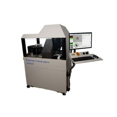
This IVS 220 model offers the best Cost of Ownership for the most advanced technology measurement capabilities up to 200mm wafer size manufacturing factories. With a TPUT of 165 wafers per hour, under 1 nanometer precision 3 Sigma and 1 nanometer of TIS, the IVS 220 system is designed to meet today’s most advanced metrology needs.
The system uses the Image Base Overlay (IBO), and can measure critical dimension (CD), overlay registration (RG), Vernier, VIAS or bump diameters, height, and even slopes for measure of all patterns drawn under the resin layer in photolithography. IVS220 is designed to qualify technological levels up to 65nm for semiconductor factories but also to fulfill the need in flexibility in compound semiconductor industries with several substrates like SiC, InP, GaN and GaAs.
The system uses the proven basement of the IVS200 system to cover the multiple range of customer demands. From a famous and a reliable base, we have added high technology items such as ETEL stage to push the system to its limits in terms of speed and accuracy.