
- Home
- Companies
- Agilent Technologies, Inc.
- Products
- Cary - Model 620 - FTIR Microscopes & ...
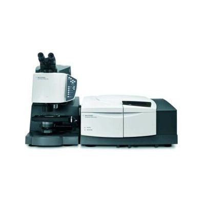
Cary - Model 620 -FTIR Microscopes & Imaging Systems
The Agilent Cary 610 and Cary 620 FTIR Microscopes and Chemical Imaging systems represent the latest in cutting-edge performance. Leveraging off the latest in technological developments, the systems now deliver unparalleled spatial resolution and sensitivity, which coupled with a wide range of options, provide flexibility to suit applications ranging from routine measurements to cutting-edge analytical development. The Cary 610 is a single point FTIR microscope, capable of mapping, while the Cary 620 is a Focal Plane Array (FPA) chemical imaging FTIR microscope. With the option to couple the microscope to either a research-grade Cary 660 FTIR or top of the range, air bearing, Cary 670 FTIR spectrometer, you get two instruments in one – a research FTIR spectrometer and an FTIR microscope. The Cary 610 microscope can be upgraded to a Cary 620 at a later date, giving flexibility for when application needs change.
- Achieve spatial resolution and data quality comparable with that of a synchrotron with Agilent’s innovative, high magnification optics.
- The Agilent 600 series instruments deliver over 400% more energy than any other FTIR system, ensuring the highest quality data with details you may never have seen before.
- A unique 4x IR objective ensures that small features can be quickly and easily detected over a large area without moving the sample – all within minutes.
- Use Agilent’s unique “Live ATR Imaging mode” to measure delicate samples in minutes by eliminating time-consuming, sample preparation techniques such as resin embedding.
- Materials applications include defect analysis of polymers, coatings and thin films.
- Detect subtle chemical changes, without staining, in tissues and cells, allowing improved and earlier disease detection.
- Measure live cells in water.
- Identify defects in semiconductor wafers and electronic components.