
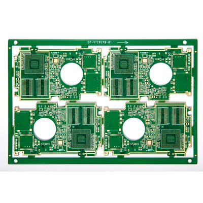
HDI PCBs
The full name of HDI PCBs is High Density Interconnector Printed Circuit Board that features a higher wiring density per unit area more than conventional printed boards. Appropriately used in high-layer count and fine laminated boards, HDI PCBs have sophisticated line and spaces, minor vias and capture pads, and higher density of connection pad density. HDI PCBs have great electrical performance and lighter weight and smaller size of the equipment. Therefore, the HDI circuit board has become the better option for costly laminated and high-layer count circuit board.
High-speed, small size, high-frequency, advanced technology, high-density.
Though HDI PCB has a complex manufacturing process, it has a wide range of applications. It can be used in various industries, such as electronic, medical industry. The lighter weight and small size give it appropriate reasons to be installed in miniature equipment.
HDI PCB is consumer-driven that fit for more and more delicate and sophisticated electronic equipment. Nowadays people prefer agility electronic equipment because of its convenience and lightweight. HDI PCB makes the equipment small and smart. It is thin and light, also features high-end technology, and high-speed operation capability.
HDI technology is a high-end technology used to manufacture HDI PCBs. This kind of printed circuit board features high density and well performance in circuit interconnection, so people also known it as high density interconnect PCB. Nowadays, HDI printed circuit boards has become one of the fastest growing technologies in printed circuit board industry.
According to the vias, HDI boards can be divided into 6 different types:
- Face to face through vias
- Through vias and buried vias
- Two or more layer with through vias
- Non-electrical connection and passive substrate
- Coreless construction with layer pairs
- Alternate constructions of coreless constructions with layer pairs
HDI Printed Circuit Board Manufacturing
An advanced HDI technology is included of via in pad process, via fill technology, non-conventional HDI PCB building, and laser drill technology.
Via in pad process: in this process, HDI PCB manufacturers place bias on the surface of the flat lands, and fill the vias with conductive or non-conductive epoxy, then capped and plated over. Finally make the via invisible.
Via fill technology: professional HDI printed circuit board manufacturers will select the most appropriate materials for the PCB. Generally speaking, silver filled, conductive epoxy, non conductive epoxy, electrochemical plating, and copper filled are the suitable fill materials for HDI PCBs.
Non-conventional HDI PCB building: HDI PBCs must combine more lines and annular ring on a thin, high-density board. Therefore to create an advanced HDI PCB should make lots of efforts on the board design and manufacturing equipment.
Laser drill technology: using a laser beam of light 20 microns in diameter can create the smallest vias on the surface of HDI PCBs. This high-energy light is precise and efficient that can cut through metal and glass to make the tiny via hole.