

- Home
- Companies
- Attolight AG
- Products
- Attolight Allalin - Hybridized ...
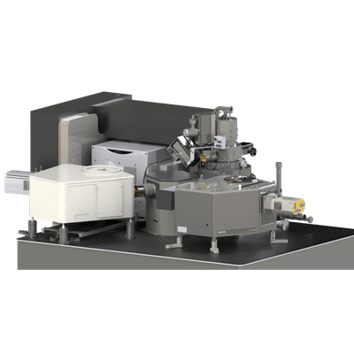
Attolight Allalin - Hybridized SEM-Spectroscopic Instrument
The Allalin is a nanometer resolution spectroscopy instrument that utilizes a patented optical collection objective integrated within the SEM column. This versatile platform supports a wide range of spectroscopic analyses through its multiple sources, including electronic and laser modes (continuous or pulsed), and various detectors such as PMT, CCD/Streak cameras, TCSPC/ADP, and Raman detectors. It can accommodate small samples from a few micrometers to wafers up to 6 inches and operates at temperatures from room temperature down to 10K, facilitated by an integrated Helium cryostat with copper braid coupling. This system can be equipped with options like an EBIC system, nanoprobes, and an HV transfer unit. Applications of the Allalin include exciton diffusion, GaN physics, nanorod and nanowire studies, plasmonics, laser diode aging, defect analysis, and substrate quality control. It is also used in the development of photovoltaic materials and other semiconductor research, supporting a wide range of materials including III-V and II-VI semiconductors and perovskites.
The Allalin is a nanometer resolution spectroscopy instrument, based on a unique and patented system including an optical collection objective integrated within the SEM column.
One platform, multiple possibilities of measurements
This platform offers a very large range of spectroscopic analysis thanks to its multiple sources (electronic, laser in continuous or pulsed mode) and many types of detectors (PMT, CCD/Streak cameras, TCSPC/ADP… detectors, Raman…). In addition, the system can be equipped with various options such as : EBIC system, nanoprobes, HV transfer unit and can welcome small samples from few µm size to wafers up to 6 inches.
The spectroscopic analyses can be conducted at any temperature from RT down to 10K thanks to an integrated Helium cryostat and copper braid coupling ensuring high stability and very low drift.
The base system is a SEM – spectroscopic platform on which multiple options can be adapted:
Sources
- Continuous/pulsed electronic source
- Continuous/pulsed laser
Spectrometers
- up to 2 spectrometers on the platform
Detectors
Continuous detectors
- PMT
- UV-Visible (EM-)CCD camera (from 180nm to 1050nm)
- InGaAs detector (from 900 to 2200nm)
Time-resolved detectors
- Streak camera
- TCSPC detector
Stages
- Nano-positioning stage (cryo-compatible)
- 3’/6’ wafer stage
Options
- Nanoprobes (up to 4 probes)
- Raman line
- EBIC/EBAC
- Electronics & optoelectronics (GaN, InP, SiC…)
- Photovoltaic cells (GaAs, CdTe, Perovskites…)
- Light emitting diodes (MicroLEDs)
- 2D materials (Graphene, BN, WS2…)
- Noble metals (plasmonic)
- Nano-micro particles
- Nano-micro wires/rods
- Photonic crystals
- Quantum wells & quantum dots
- Minerals, glasses, ceramics and gemstones
- Inorganic coatings
- Polymers layers
- Organic materials
- Biological samples, cells, vesicles