

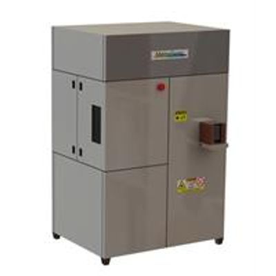
MetroDefect - Model 301 -Wafer Defect Inspection System
2D imaging technology provides fast, reliable inspection for defects down to one micron. Metrosemi`s Truebump Technology combines multiple 3D metrology techniques to deliver 100% bump height. This new technology is the foundation of Metrosemi’s products designed to offer fast throughput, increased brightfield and darkfield sensitivity and solves site alignment challenges for large die. The MetroDefect® 301 system now offers Clearfind Technology for non-visual residue detection. The MetroDefect 301 system is tightly integrated with control and analytical software for real-time analysis and review, IR defect review, while also providing offline review options. When massive amounts of bump data are generated during inspection, users now have the analytical tools to visualize data, correct process variations and improve yields.
Combining 2D and 3D technologies to detect yield-robbing defects and measure features critical for today`s packaging technology, the MetroDefect® 301 will reset the industry`s expectations for throughput, accuracy and reliability.
- Bumping
- After develop and etch
- Large die, multi-chip packages
- Reconstituted wafers
- Redistribution layers
- OQA and post saw
- Gel and waffle pack inspection
- Multi-product, multi-grid
- Inline real-time focusing
- Flexible platform to allow for metrology sensor integration
- IR defect review (option)
- Integrated review and analysis (option)
- Large die and package support (>1000sq mm2)
- Substrate support: 100mm 330mm wafers