

Metrosemi products
Thickness Measurement
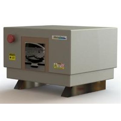
MetroThick - Model 201 - Film Metrology System
The MetroThick 201 film metrology system helps achieve strict process tolerances at sub-7nm logic and leading-edge memory design nodes by providing high-precision thin film measurements for a broad range of film layers. The high brightness light source drives the spectroscopic ellipsometry technology which provides the signal required to accurately measure the bandgap and provide insight into electrical performance weeks earlier than e-test. New FoG™ (Films on Grating) algorithms further increase the measurement’s correlation to device by enabling film measurement on a device-like grating structure. With increased throughput, MetroThick 201 offers high productivity, supporting the increased number of film layers associated with leading-edge device fabrication techniques.
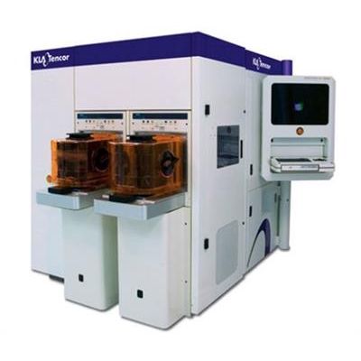
Aleris - Model 8500 - Film Metrology System
KLA-Tencor`s New Aleris 8500 Film Metrology System is Industry`s Most Advanced Thickness and Composition Measurement Technology for 45nm and BeyondSAN JOSE , Calif. , — December 03, 2007 — KLA-Tencor (NASDAQ: KLAC) introduced the Aleris family of films metrology systems, beginning with the Aleris 8500 which is the industry’s first system to combine production-worthy composition and multi-layer film thickness metrology.
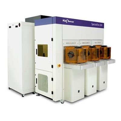
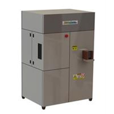
SpectraFilm - Model F1 - Film Metrology System
The SpectraFilm F1 film metrology system helps achieve strict process tolerances at sub-7nm logic and leading-edge memory design nodes by providing high-precision thin film measurements for a broad range of film layers. The high brightness light source drives the spectroscopic ellipsometry technology which provides the signal required to accurately measure the bandgap and provide insight into electrical performance weeks earlier than e-test. New FoG™ (Films on Grating) algorithms further increase the measurement’s correlation to device by enabling film measurement on a device-like grating structure. With increased throughput, SpectraFilm F1 offers high productivity, supporting the increased number of film layers associated with leading-edge device fabrication techniques.
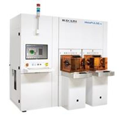
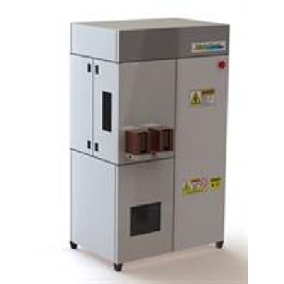
MetaPULSE - Model G - Metal Films System
The MetaPULSE Series is the industry standard for thickness measurements of metal films. The MetaPULSE G System delivers superior performance on all metal films, and is optimized for thin single and multilayer applications that are critical in advanced logic, memory and 3D packaging processes. Rudolph`s patented PULSE™ Technology offers a non-contact, non-destructive technique to measure the thickness of each layer in a multi-layer metal film stack on product wafers, without interference from underlying layers or levels. Unlike optical and x-ray techniques, PULSE Technology measures film thickness using a time-resolved acoustic signal that can be used in active die without the requirement for special metrology test sites.
Wafer Stress Measurement
MetroStress - Model 101 - Semiconductor Wafer Stress Measurement
Faced with the increasing complexity of semiconductor manufacturing processes, IDMs and foundries rely on high performance production-worthy transparent film metrology for fabwide process control. Metrosemi’s MetroStress 101 of metrology systems deliver superior measurement accuracy, repeatability and tool-to-tool matching on a highly reliable and flexible platform. Utilizing Metrosemi’s patented focused beam laser ellipsometry (FBE) system with optional deep ultraviolet reflectometry, visible reflectometry, the MetroStress 101 System has been qualified to provide on-product process control for logic and memory processes down to the 1x node.
Metrosemi - Model FLX 2320S - Wafer Stress Laser Scanner
The FLX-2320-S determines stress by measuring the curvature change of pre- and post- film deposition. It can measure film stress from -65ºC to 500ºC at a heating rate up to 30ºC/min. Stress variation with temperature is able to be used to characterize film properties, such as moisture concentration, phase changes, thermal expansion, volume changes, and plastic deformations. Other characteristics of the instrument include: – Dual wave lengths – Calculation of biaxial modules of elasticity, linear expansion coefficient, stress uniformity and file subtraction – Calculation of water diffusion coefficient – 2-D and 3-D view of wafer topography – Wafer size: 75 – 200 mm – Measurement temperature: from -65ºC to 500ºC – PC base controller – Speed: 5 sec for 150 mm wafer – Minimum scan step: 0.02 mm – Maximum points per scan: 1250
Wafer Defect Inspection
MetroDefect - Model 301 - Wafer Defect Inspection System
2D imaging technology provides fast, reliable inspection for defects down to one micron. Metrosemi`s Truebump Technology combines multiple 3D metrology techniques to deliver 100% bump height. This new technology is the foundation of Metrosemi’s products designed to offer fast throughput, increased brightfield and darkfield sensitivity and solves site alignment challenges for large die. The MetroDefect® 301 system now offers Clearfind Technology for non-visual residue detection. The MetroDefect 301 system is tightly integrated with control and analytical software for real-time analysis and review, IR defect review, while also providing offline review options. When massive amounts of bump data are generated during inspection, users now have the analytical tools to visualize data, correct process variations and improve yields.
Metrosemi - Model 3900 Series - Wafer Defect Inspection and Review Systems
In advance of SEMICON West, KLA-Tencor Corporation (NASDAQ: KLAC) was introduced advanced wafer defect inspection and review systems for leading-edge IC device manufacturing: the 3900 Series (previously referred to as Gen 5) . This system employ a range of innovative technologies to form a comprehensive wafer inspection solution that enables discovery and control of yield-critical defects at all stages of IC manufacturing— from early process characterization to production process monitoring.
SECS/GEM Automation
MetroSecs/Gem - Model 401 - Wafer Panel Automation
The platform, configurable for either wafer (round) or panel (rectangular) substrates, offers multiple imaging modes, including Clearfind® Technology, a technique for enabling a large process window to detect residue defects on metal and metal defects on organic layers. The combination of substrate flexibility, defect sensitivity and metrology in a single platform reduces capital investment requirements and provides a reliable pathway to transition from wafer to panel-based processes for applications requiring high I/O counts and multiple-chip integration, such as SoC with memory, wireless module and wide I/O memory. Integration with Discover Defect software quickly turns defect data into actionable process control, improves classification and reduces manual review. It enables our customers to develop, learn and analyze new processes reliably while significantly improving their product delivery time to market.