

Metrosemi
MetroStress - Model 101 -Semiconductor Wafer Stress Measurement
FromMetrosemi
Faced with the increasing complexity of semiconductor manufacturing processes, IDMs and foundries rely on high performance production-worthy transparent film metrology for fabwide process control. Metrosemi’s MetroStress 101 of metrology systems deliver superior measurement accuracy, repeatability and tool-to-tool matching on a highly reliable and flexible platform. Utilizing Metrosemi’s patented focused beam laser ellipsometry (FBE) system with optional deep ultraviolet reflectometry, visible reflectometry, the MetroStress 101 System has been qualified to provide on-product process control for logic and memory processes down to the 1x node.
Most popular related searches
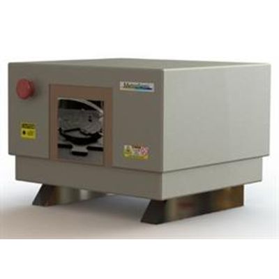
- Product Name: MetroStress 101
- Client: Metrosemi
- Wafer diameters: 200 mm (8 in), 150 mm (6 in), 100 mm (4 in).
- Substrate temperature range: -65 °C to 500 °C.
- Stress Range: 1 MPa to 4 GPa.
- Scan rate: 6 seconds per scan.
- Repeatability: 1 MPa.
- Resolution: 1 MPa.
- Ultrathin Gates
- Oxides, Nitrides
- Single and multilayer dielectrics
- Thin metals (<100Å)
- Hardmask layers
- ARC/BARC
- SiGe
- SOI
- Polysilicon
- Resists
- Thick Films
- Etch rate and CMP monitoring
- Film stress and wafer bow