

- Home
- Companies
- k-Space Associates, Inc.
- Products
- Model MOS UltraScan/ThermalScan - ...
Model MOS UltraScan/ThermalScan -Full-Sample Mapping of Curvature, Stress, Tilt, and Bow Height
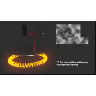
The kSA MOS UltraScan and kSA MOS ThermalScan systems are ex situ, flexible, high-resolution scanning wafer curvature, bow, and tilt-measurement systems. The kSA MOS UltraScan and kSA MOS ThermalScan systems are flexible, high-resolution scanning wafer curvature, bow, and tilt-measurement systems. Based on proven and patented kSA MOS technology, the kSA MOS UltraScan uses a laser array to map the two-dimensional curvature, wafer bow, and stress of semiconductor wafers, optical mirrors, glass, lenses – practically any polished surface. For room temperature measurements, explore the kSA MOS UltraScan. If you want to know how your wafer changes with temperature, explore the kSA MOS ThermalScan.
The kSA Multi-beam Optical Sensor, or kSA MOS, technology is based on a patented approach which uses a single laser to generate a two-dimensional laser array. This laser spot array is then reflected off the sample surface into a high-resolution camera. Changes in the reflected laser array spot spacing at each point on the sample are used to determine the localized wafer curvature in both the X and Y direction. In this way, the system directly measures the curvature and stress in two dimensions simultaneously. This is something that single or dual beam curvature and stress tools simply
Simultaneous detection of the laser array also makes the measurement inherently less sensitive to sample vibration compared with systems that rely on scanning the laser spot on the surface of the sample to measure the local curvature. This leads to kSA MOS’s increased wafer curvature resolution capability. Since all the laser spots move together at the same frequency, movement or tilt is not incorrectly detected as a change in sample curvature. Through the use of sophisticated image processing and data analysis algorithms, the kSA MOS UltraScan can easily detect micron-sized changes in spot position due to curvature changes, which translates to the highest wafer curvature/stress resolution metrology tool available.
kSA MOS UltraScan is equipped with XY scanning over a 300mm x 300mm area. This provides the advantage of uniform spatial data resolution over the entire sample (wafer, mirror, or other reflective surface). At large diameters spatial resolution will not be lost, which is typically a problem in linear scanning systems with rotation stages. It also provides easy measurement set up for rectangular samples or for mapping limited areas of a sample.
kSA MOS UltraScan is equipped with both flat and curved reference mirrors for quick and easy curvature calibration. The curvature of your wafer (or other reflective surface) is measured directly from the laser spot spacing, resulting in high accuracy single point and scanning curvature measurements. Using sophisticated image processing and data analysis algorithms, the kSA MOS UltraScan can easily detect sub-micron changes in spot position due to changes in sample curvature. This makes it the highest wafer curvature and stress resolution metrology tool available.
Absolute reflectance of the wafer (or other sample) at the laser wavelength is determined by measuring the integrated intensity of the laser spots on the camera , and is automatically calibrated before each scan by using the integrated flat mirror. This provides useful information about the quality and uniformity of the sample surface, as well as interference effects for film stacks.
When a laser is reflected off a bowed sample, the reflected angle will differ at different points on the wafer (or other sample). The automated laser tracking in the kSA MOS UltraScan optics not only keeps the laser array centered on the detector but also measures the changes in the angle of reflection of the laser array in order to determine the local wafer bow height and surface tilt angle.
To generate a thin-film stress map of a wafer, the local curvature of the wafer must be determined both pre- and post-deposition. The point-by-point thin-film stress is determined based on the change in the point-by-point curvature from the pre- and post-process curvature maps, as well as the substrate thickness, the biaxial modulus of the substrate and the film thickness. The changes in stress of a thin film after processing may also be determined from the wafer curvature maps measured after the subsequent processing steps.
This option equips the kSA MOS UltraScan optics with a light source and a fiber coupled spectrometer. This allows the spectral reflectance of the wafer (or other sample) to be measured at each point on the sample. Using kSA’s proprietary software to measure the extrema positions in the spectral reflectance spectra, the kSA MOS UltraScan can determine the point-by point thickness of semitransparent thin films on a substrate. This data can be mapped along with other measurement parameters such as wafer curvature and film stress. Alternatively, the spectral reflectance data can be exported for multi-layer thickness or device modeling in other software programs.