

- Home
- Companies
- Thermo Fisher Scientific, LIMS & ...
- Products
- Helios - Model 5 PXL PFIB Wafer ...
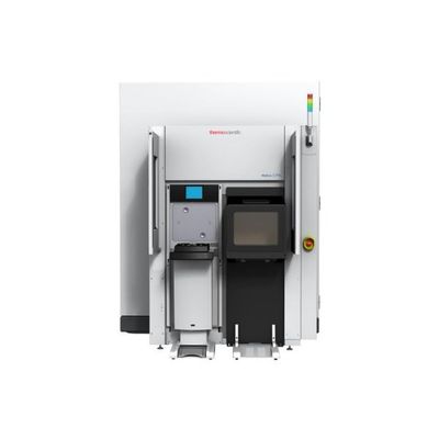
Helios - Model 5 PXL PFIB Wafer DualBeam -Plasma Focused Ion Beam Scanning Electron Microscope (PFIB SEM)
PFIB SEM for in-line metrology and process monitoring of advanced 3D NAND and DRAM devices. The Thermo Scientific Helios 5 PXL Wafer DualBeam is a plasma focused ion beam scanning electron microscope (PFIB SEM) that redefines the standard for high-aspect-ratio through-stack metrology and structural verification. It features high-performance in-line metrology and process monitoring to quickly provide critical insights for process development and manufacturing engineers. Designed to meet the in-line metrology and process control requirements of the fab, the Helios 5 PXL Wafer DualBeam significantly reduces time to data and enables the wafer to be returned to the line without being pulled and scrapped. The Helios 5 PXL Wafer DualBeam is compatible with semiconductor factory automation, facilitating operator-free recipe-driven operations. This automation can support the high-throughput requirements of fab metrology and process monitoring – even on the most challenging structures.
Utilizing the patented Thermo Scientific Elstar Electron Column with the high-performance PFIB2.0 xenon plasma ion column, the Helios 5 PXL Wafer DualBeam delivers high-resolution, high-contrast imaging. Obtain exact dimensional measurements of high-aspect-ratio 3D through-stack structures, data that is not easily accessible to conventional in-line metrology tools.
Fast, precise, large-area wafer level deprocessing, diagonal milling and cross sectioning of high-aspect-ratio structures. Advanced automation capabilities identify potential issues, accelerating process development and minimizing manufacturing disruptions.
The Helios 5 PXL Wafer DualBeam is backed by our world-class service, knowledge, and expertise in advanced metrology sample preparation and failure analysis.
Xe+ Plasma FIB Column
- PFIB beam current from 1 pA to 2.6 µA
- Inductively coupled Xe+ plasma (ICP) >4000 hours
Elstar UHR Immersion Lens FESEM Column
- Elstar electron gun with ultra-stable Schottky field emitter gun with UC+ monochromator technology
- Electron beam resolution:
- 0.9 nm @ 15 kV
- 1.0 nm @ 1 kV
- Electron source lifetime: 12 months
Gas delivery
- Thermo Scientific MultiChem Integrated Gas Delivery System
- Slots for up to 6 chemistries
- Single gas injection system
- Port for up to 3 independent GIS units
Wafer handling
- Automated handling of 300 mm FOUP with EFEM (GEM300 compliant)
- Manual loading of 300 mm, 200 mm & 150 mm wafers
Additional options
- CAD navigation compatibility (NEXS and Synopsys Camelot)
- Retractable directional backscatter detector (RDBS)*
Modern data demands are driving innovation in 3D NAND, DRAM and other memory structures. Our memory analysis tools and workflows offer high-productivity characterization so that manufacturers can meet performance, latency, and capacity demands.
Semiconductor Pathfinding and Development
Advanced electron microscopy, focused ion beam, and associated analytical techniques for identifying viable solutions and design methods for the fabrication of high-performance semiconductor devices.
We offer advanced analytical capabilities for defect analysis, metrology, and process control, designed to help increase productivity and improve yield across a range of semiconductor applications and devices.
Semiconductor Failure Analysis
Increasingly complex semiconductor device structures result in more places for failure-inducing defects to hide. Our next-generation workflows help you localize and characterize subtle electrical issues that affect yield, performance, and reliability.
Physical and Chemical Characterization
Ongoing consumer demand drives the creation of smaller, faster, and cheaper electronic devices. Their production relies on high-productivity instruments and workflows that image, analyze, and characterize a broad range of semiconductor and display devices.
ESD Semiconductor Qualification
Every electrostatic discharge (ESD) control plan is required to identify devices that are sensitive to ESD. We offer a complete suite of test systems to help with your device qualification requirements.