
Applied Materials, Inc. products
Semiconductor

Applied - Model Aera4 - Mask Inspection System
The Applied Aera4 Mask Inspection system is a fourth-generation 193nm-based inspection tool unique in combining true aerial imaging with cutting-edge high-resolution imaging. Equipped with a new lithography-grade lens, the Aera4 system demonstrates improved signal-to-noise for both standard high-resolution applications and aerial inspection, making it the tool of choice for 1x nm technology nodes and for early-production EUV mask inspection. The system performs highly sensitive mask inspection, as required for double- and quadruple-patterning lithography technologies, while maintaining a very low false alarm rate.

Nokota - Model ECD - Electrochemical Deposition Systems
The Nokota system expands the Applied Materials suite of electrochemical deposition systems with a high-productivity wafer-level packaging tool that delivers best-in-class performance for the full range of plating steps used in diverse packaging schemes. These range from flip chip and wafer-level chip-scale packages to 2D and 3D fan-out, 2.5D interposerdesigns, and through-silicon via. Systems are available for 150mm, 200mm, and 300mm operation, and for simultaneous processing of 150mm/200mm and 200mm/300mm wafers. Copper, tin/silver alloy, nickel, gold, tin, and palladium are the metals most commonly used, although others can be accommodated.
Screen Printing Systems
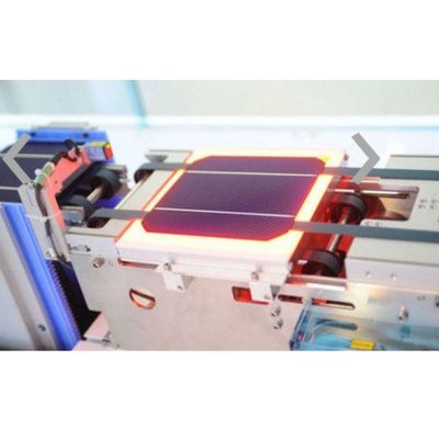
Applied - Baccini Soft Line
The Applied Baccini Soft Line is an integrated, fully automated line for crystalline silicon PV cell production. The line features Baccini’s advanced screen printers and drying ovens for back contact, bus bar and front contact metallization, and inspection systems that check print quality. In addition, the line also comes equipped with a laser system for edge isolation to prevent back contact shunt and a tester-sorter for testing and distributing cells according to their efficiencies.

Applied Tempo - Metallization System
The Tempo screen printer sets a new standard in cell manufacturing, supporting fast ramp time to production, a proven industry-record output of more than 75,000 wafers per day and the highest yields of high-efficiency cells. The Tempo system is Applied Materials’ highest productivity platform for crystalline silicon PV cell production. The new metallization platform addresses industry demand for high productivity at the lowest cost per watt, processing more than 3,200 wafers per hour at greater than 92% uptime. Capable of supporting industry-leading Applied Fine Line Double Print™ technology, the new integrated metallization and test & sort platform produces high-efficiency cells at high yields with minimal fine line “finger” interrupts. Extendable to advanced cell architectures, the Tempo metallization system is designed to support current and future industry roadmaps for cell efficiency and cost targets.
Wafering and Inspection

Applied Vericell - Solar Wafer Inspection System
The Applied Vericell Solar Wafer Inspection System is the industry’s most advanced fully automated bare wafer inspection tool for crystalline silicon PV wafer and cell production. The Applied Vericell system’s multiple integrated inspection modules automatically evaluate each wafer to find and eliminate defective wafers from production, resulting in significant manufacturing savings. The Vericell measures and reports on a wide range of parameters including wafer thickness, thickness variations, warp and resistivity. Vericell also detects defects including saw marks, chipped edges, damaged chamfers, stains, pin holes and micro-cracks.