
Physical Electronics, Inc. (PHI) products
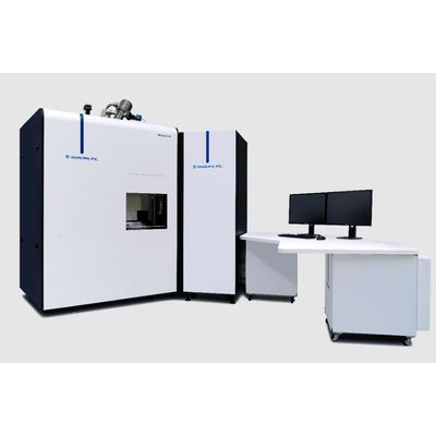
Quantes - Model XPS/HAXPES - Scanning Microprobe
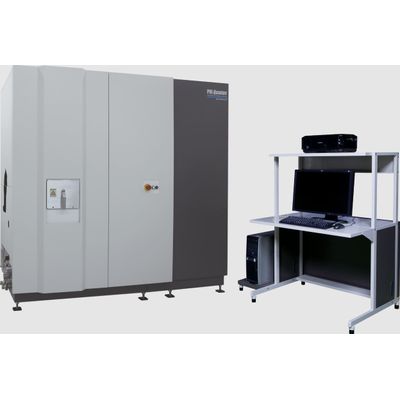
PHI - Model PHI 710 - Scanning Auger Nanoprobe
The PHI 710 Scanning Auger Nanoprobe is a unique, high performance Auger Electron Spectroscopy (AES) instrument that provides elemental and chemical state information from sample surfaces and nano-scale features, thin films, and interfaces. Designed as a high performance Auger, the PHI 710 provides the superior Auger imaging performance, spatial resolution, sensitivity, and the spectral energy resolution needed to address your most demanding AES applications.
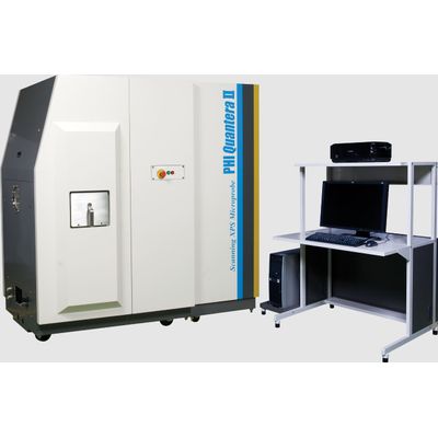
PHI Quantera - Model II - Scanning XPS Microprobe
The core technology of the Quantera II is PHI’s patented, monochromatic, micro-focused, scanning x-ray source which provides excellent large area and superior micro-area spectroscopy performance. Spectroscopy, depth profiling, and imaging can all be performed over the full range of x-ray beam sizes including the minimum x-ray beam size of less than 7.5 µm. In addition to superior XPS performance characteristics the Quantera II provides two in situ sample parking stations which enables the automated analysis of all three sample platens in a single user defined analysis queue.
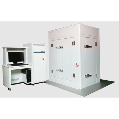
PHI nanoTOF - Model 3 - Mass Spectrometers
PHI’s patented TRIFT mass spectrometer with Parallel Imaging MS/MS provides superior sensitivity, low spectral background, unique ability to image highly topographic surfaces, high mass accuracy and mass resolution, and unambiguous high mass peaks identification with parallel tandem MS imaging capability. The nanoTOF II can be configured with a wide variety of options to optimize performance for organic materials, inorganic materials, or both, depending on customer requirements.
PHI - Model TOF-SIMS - Time-of-Flight Secondary Ion Mass Spectrometry
Time-of-Flight Secondary Ion Mass Spectrometry (TOF-SIMS) provides elemental, chemical state, and molecular information from surfaces of solid materials. The average depth of analysis for a TOF-SIMS measurement is approximately 1 nm. Physical Electronics TOF-SIMS instruments provide an ultimate spatial resolution of less than 0.1 µm.
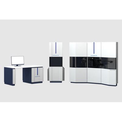
PHI - Model VersaProbe 4 - Scanning XPS Microprobe
The PHI VersaProbe 4 is a highly versatile, multi-technique instrument with PHI’s patented, monochromatic, micro-focused, scanning X-ray source. The instrument offers true SEM-like ease of operation with superior micro area spectroscopy and excellent large area capabilities. The fully integrated multi-technique platform of the PHI VersaProbe 4 offers an array of optional excitation sources, sputter ion sources, and sample treatment and transfer capabilities. These features are essential in studying today’s advanced materials and in supporting your material characterization and problem-solving needs. The new PHI VersaProbe 4 has improved spectroscopic performance, new large area imaging and mapping capabilities, and environmentally friendly modern configuration with efficient power consumption, faster pump-down and ergonomic design.
Haxpes
The basic principle of hard x-ray photoelectron spectroscopy is similar to that of general XPS, in which a sample is irradiated with photons, and the count and kinetic energy of emitted photoelectrons is measured. While the photon energy of the monochromatic Al Kα x-ray source most commonly used in traditional XPS instruments is 1486.6 eV, the photon energy of the excitation source used in hard x-ray photoelectron spectroscopy is 5 to 8 keV, more than triple. “Hard x-ray photoelectron spectroscopy” is abbreviated as HX-PES or HAXPES. HAXPES is traditionally performed at synchrotron facilities.
Auger Electron Spectroscopy (AES)
Auger Electron Spectroscopy provides quantitative elemental and chemical state information from surfaces of solid materials. The average depth of analysis for an AES measurement is approximately 5 nm. Physical Electronics Auger instruments provide the ability to obtain spectra with a lateral spatial resolution as small as 8 nm. Spatial distribution information is obtained by scanning the micro focused electron beam across the sample surface. Depth distribution information is obtained by combining AES measurements with ion milling (sputtering) to characterize a thin film structure. The information AES provides about surface layers or thin film structures is important for many industrial and research applications where surface or thin film composition plays a critical role in performance including: nanomaterials, photovoltaics, catalysis, corrosion, adhesion, semiconductor devices and packaging, magnetic media, display technology, and thin film coatings used for numerous applications.