
Scientific Computing International products
Semiconductor
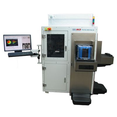
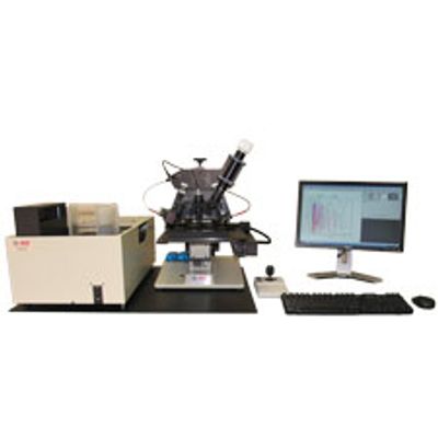
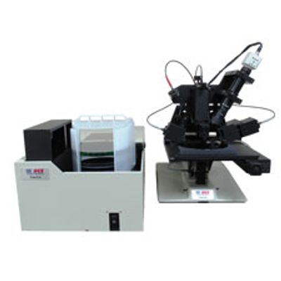
Model FilmTek 6000 PAR-SE - Optical Thin-Film Metrology for Advanced Thin Films
The FilmTek™ 6000 PAR-SE is our most advanced film metrology system for film thickness, refractive index and stress measurement for a broad range of film layers at the 1x nm design node and beyond. The FilmTek™ 6000 PAR-SE accommodates 200 or 300 mm wafer metrology. The FilmTek™ 6000 PAR-SE combines spectroscopic ellipsometry and DUV multi-angle polarized reflectometry with a wide spectral range to meet the challenging demands associated with multi-patterning and other leading-edge device fabrication techniques. Manufacturing advanced IC devices at 1x nm design rules requires the use of complex films that must be highly uniform. To maintain tight control over the processes used to build these films requires metrology systems that can monitor extremely thin films that are often within a multi-layer film stack (e.g., high-k and oxide-nitride-oxide films).
Model FilmTek CD - Optical Critical Dimension (OCD) and Advanced Film Analysis Metrology
The FilmTekTM CD optical critical dimension system is SCI’s leading-edge solution for fully-automated, high-throughput CD measurement and advanced film analysis for the 1x nm design node and beyond. This system delivers real-time multi-layer stack characterization and CD measurement simultaneously, for both known and completely unknown structures. FilmTekTM CD utilizes patented multimodal measurement technology to meet the challenging demands associated with the most complex semiconductor design features in development and production. This technology enables measurement of extremely small line widths, with high accuracy measurements in the sub-10nm range.
Advanced Packaging & TSV
Model FilmTek 2000M TSV - Advanced Semiconductor Packaging – TSV Metrology
The FilmTek™ 2000M TSV advanced semiconductor packaging metrology system provides an unmatched combination of speed, accuracy, and precision for high-throughput measurements of resist thickness, through silicon vias (TSVs), Cu-pillars, bumps, redistribution layer (RDL) and other packaging processes. TSV etch depth and depth uniformity is critical to ensure high yield during TSV fabrication. The FilmTek™ 2000M TSV can readily determine etch depth for via structures with diameters greater than 1 µm up to a maximum etch depth of 500 µm. Additional capabilities include measurement of height or depth, critical dimension, and film thickness for microbumps, trenches, and a variety of other structures and applications.
Photonics & Telecom
Model FilmTek 4000 - Multiple Angle Reflectometry
The FilmTek™ 4000 metrology system offers fully-automated wafer metrology optimized for photonic integrated circuit manufacturing. This system offers several advances designed to enable optical component manufacturers to increase functional yield of their products, reliably and at lower cost. Utilizing multi-angle reflectometry and patented multi-angle Differential Power Spectral Density analysis capability, the FilmTek™ 4000 delivers unmatched measurement accuracy required to meet waveguide manufacturing specifications. Measurement resolution is optimized through independent thickness and index (TE and TM modes) measurements of each cladding and core layer, with index measurement resolution up to 2×10⁻⁵. This provides a 100x performance advantage over the best non-contact method and 10x that of the best prism coupler contact systems.
Model FilmTek 3000 PAR-SE - Combined Ellipsometry and Micro-spot DUV-NIR Reflection/Transmission Spectrophotometry
The FilmTek™ PAR-SE combined metrology line is our most advanced metrology solution, with the highest accuracy, precision, and versatility in the industry. The FilmTek™ 3000 PAR-SE was engineered to meet the needs of any advanced thin film measurement application, and excels at material characterization on both transparent and non-transparent substrates. The FilmTek™ 3000 PAR-SE combines spectroscopic ellipsometry, DUV multi-angle polarized reflectometry, and transmission measurement with a wide spectral range to meet the most challenging of measurement demands in both R&D and production. SCI’s patented parabolic mirror technology allows for a small spot size down to 50µm, ideal for direct measurement of product wafers and patterned films.