

Tokyo Electron Limited (TEL) products
Coater/Developers - LITHIUS Series
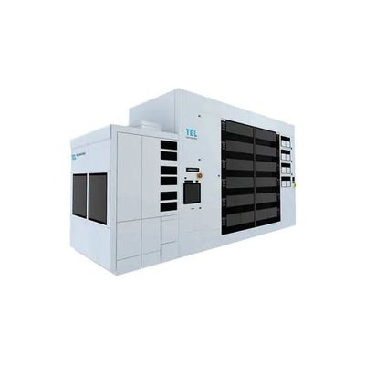
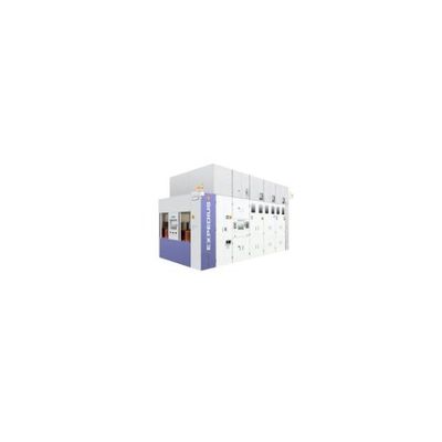
Clean Track Lithius - Model Pro Z - Automated Monitoring System
CLEAN TRACK™ LITHIUS Pro™ Z is TEL`s most advanced 300mm coater/developer for the 10nm technology node and beyond. It incorporates user-friendly operation, flexible configurations for future processes, and automated monitoring technology to support a wide range of applications from next generation development to high volume mass production. Compared to the previous generation LITHIUS Pro™ and Pro V, the LITHIUS Pro™ Z improves performance in three key areas - defectivity, productivity, and CoO (Cost of Ownership). CLEAN TRACK™ LITHIUS Pro™ Z offers increased process flexibility to support advanced immersion lithography, including double and multiple patterning schemes as well as EUV process.
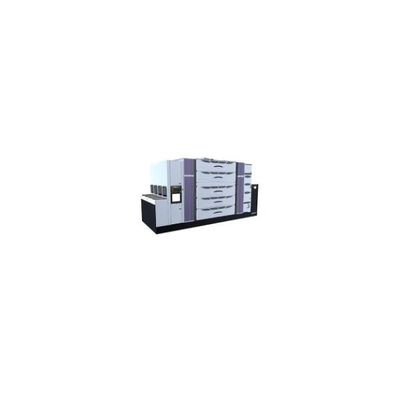
Clean Track - Model Lithius Pro V/Lithius Pro V -i - Clean Track Coater
CLEAN TRACK™ LITHIUS Pro™ V incorporates all of the advanced technology of the proven CLEAN TRACK™ LITHIUS Pro™ V. It enables higher throughput, increases wafers per day, and improves overall equipment efficiency. Additionally, it also meets industry requirements for versatile lithography equipment capable of leading edge processes, including double patterning.
Surface Preparation Systems - Cellesta Series
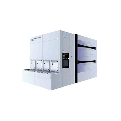
Cellesta - Model i MD - Single Wafer Cleaning System
The CELLESTA™ -i MD is a TEL`s most advanced 300mm single wafer clean system for 10nm technology node and beyond. The system has state-of-the-art cleaning capability which enables damage less clean of the well-patterned wafer surface and damage free particle removal. Pattern collapse free drying technology is also realized by implements of both chamber atmosphere control and performance improvement of IPA dispenser. The system has achieved higher productivity and lower running cost with the use of newly developed chemical recycle concept. The CELLESTA™- i MD offers scalability and will strongly support the establishment of the most challenging wafer surface clean process technologies using various chemicals for Cu and other metal exposed layer of next generation devices.
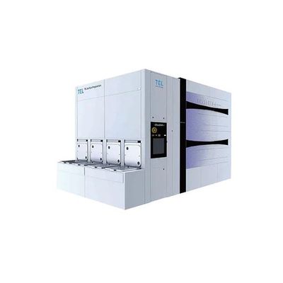
Cellesta - Model i - Single Wafer Cleaning System
CELLESTA™ -i for 300mm wafer surface clean processing system provides enhanced productivity and significantly decreased footprint. The system incorporates up to twenty units of cleaning chambers and has much smaller footprint. Furthermore, it is equipped with integrated chemical recycle technology contributing less CoO, physical cleaning function for the particle removal on wafers; all of these functions contribute to achieve higher productivity. Additionally, this platform has excellent system extendibility, which is able to equip advanced bevel clean unit dedicated to wafer periphery and backside clean unit with less chemical consumption.
Surface Preparation Systems - Expedius Series
Expedius+ - Model UW300Z - Auto Wet Station
The EXPEDIUS™ + is a 300mm batch clean system which is the advanced model of the highly reliable UW300Z EXPEDIUS™, a concept endorsed by many semiconductor manufacturers. The EXPEDIUS™ + is designed for 45nm and beyond technology node and has improved upon its predecessor in both performance and productivity. The configuration of the chemical treatment tanks, pure water rinse tanks, and dryer has been optimized to support FEOL clean, which requires particularly stringent process performance. Standard installation of the new SD2 dryer enables significant reduction of 45nm size or less micro-particles.
Test System - Cellcia Series
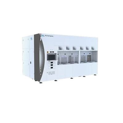
Cellcia - Multi-Cell Test System
There are an increasing variety of test requirements in conjunction with diversified device design, device application, process node shrink and package design complexity. To reduce total test cost, especially in Memory applications, multi-site probe cards were introduces as a way of reducing test cost. This method found its limit when single wafer/one-touch-down probe card technology appeared. Cellcia™ is a breakthrough technology. Splitting wafer lots into the Cellcia™ multi-cell probe system, reduces test turn-around-time and improves system footprint by adopting a multi-layer structure. Conventional prober technology cannot achieve the Cellcia™ throughput with similar floor space. The Cellcia™ system maximizes test efficiency and minimizes total test cost. TEL has combined its vast wafer probe experience and front-end process technologies to develop the world’s leading probe system, Cellcia™.