
3D-Micromac AG
- Home
- Companies
- 3D-Micromac AG
- Products
- microPREP™ - Model 2.0 - ...
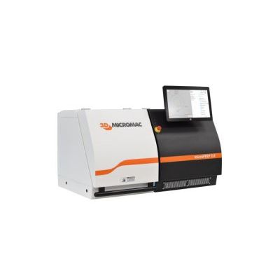
microPREP™ - Model 2.0 -High-Throughput Laser Based Microdiagnostics Sample Preparation
From3D-Micromac AG
microPREP™ 2.0 enables high-volume sample preparation of metals, semiconductors, ceramics, and compound materials for microstructure diagnostics and failure analysis. The system can be used for a variety of semiconductor sample preparation applications, including in-plane geometries and bulk samples, cross-sections, box milling for diagnostics of electrical connections and 3D chip-level structures, and full line cuts for complex investigations of complete devices. microPREP™ 2.0 complements existing approaches to sample preparation such as FIB processing and is suited for SEM inspection of avanced packaging devices, X-ray microscopy, atom probe tomography, and micro mechanical testing.
Most popular related searches
sample preparation
X-ray microscopy
high volume sampling
bulk sampling
analysis system
sample preparation system
atomic microscopy
tomography
scanning electron microscope
microscopy
- Shorter time to sample: up to 10 000 times faster than FIB
- Up to an order of magnitude lower CoO
- High degree of automation due to recipe-based, ergonomic user interface
- Virtually no structural damage and no elemental contamination by ps laser processing
- Providing larger-sized samples with micron-level precision
- Enables the creation of samples with complicated/3D shapes (TSVs, SiP)
- Meets the essential requirements of the SEMI S2/S8