

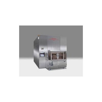
E-Beam - Model F5113 -Lithography System
Low-Cost, High Throughput EB Lithography Tool Supports Ultrafine Pattern Fabrication for Diverse Substrates. The F5113 is an electron-beam lithography system supporting 200mm and 3-inch through to 6-inch substrates, making it an optimal tool for processing advanced LSIs, compound semiconductor wafers, magnetic heads, smart power devices, photonics devices, MEMS, and other devices requiring ultrafine-pitch fabrication. The F5113`s character projection (CP) functionality offers high resolution, excellent pattern fidelity, and high throughput. High-speed pattern exposure with CP enables a broad range of applications, including materials R&D and evaluation. Advantest`s proprietary self-cleaning technology massively improves the stability of the electron beam used by the F5113, contributing to higher utilization ratios and lower customer running costs across the spectrum of applications.
- Can be easily adjusted to handle diverse substrates (inquire for details)
- High accuracy, high throughput
- Self-cleaning functionality
- Supported Substrates: 200mm, 3-inch to 6-inch
- Beam Acceleration Voltage: 50kV
- Lithography Methods: CP, VSB
- Reduction Ratio of CP Projection: 60x
- Supported Nodes: 90nm and below (Smallest node supported varies by application. Inquire for details.)